Project 2: ULNAv2-B
This project is due on Wednesday, May 17, at 11:59:59 PM
(Eastern daylight time). You must use submit to
turn in your homework like so:
submit cs411_jtang proj2 proj2.circ proj2.S
Each submitted file must contain your name and assignment
number. For the Logisim file, place that information in a text label
on the main circuit. For the assembly file, place that information
in a comment at the top of the file.
This assignment builds upon the logic components and assembly code from Homework 4, and your C code from Homework 3. Thus, you must have completed those homework assignments before attempting this assignment.
In this assignment, you will finish building the ULNAv2-B processor in Logisim. To test your processor, you will translate your fizzbuzz assembly code from Homework 2 into ULNAv2-B. Ideally your circuit implementation will match the emulator's results.
Part 1: ULNAv2-B Fizzbuzz Assembly
To begin, create a directory for your assignment and download the following files into that directory via wget:
- http://www.csee.umbc.edu/~jtang/cs411.s23/homework/proj2/proj2.S
-
Skeleton assembly code. You will re-implement
your HW2's
fizzbuzz_asmin ULNAv2-B. - http://www.csee.umbc.edu/~jtang/cs411.s23/homework/proj2/Makefile
- Builds all of the code for this assignment, by simply running make. Also included is a clean target to remove all built objects.
It is time to write the final assembly code. Take
your fizzbuzz_asm function that was originally written in
ARMv8-A in HW2. Translate it into ULNAv2-B and insert it into
proj2.S. Note that two of the function's inputs are pointer
addresses, to which store the number of fizzes and the number of
buzzes.
Assemble the binary. Test your binary in the emulator. Your implementation is correct if it calculates 0x15 fizzes and 0x0d buzzes, given the target value 0x41.
Part 2: Data Memory
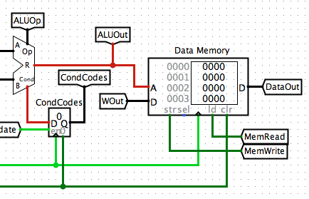
Edit your Logisim circuit proj2.circ. To your Main circuit,
add a Data Memory
(a
RAM device) component, configured with separate load and store
ports. Set the Data Memory's address width to 16 bits, and data
width also to 16 bits. Join its clock line, so that changes to data
memory occur on falling edges. For now, connect the memory's address
line to the ALU output, and input data line to WOut. Add
tunnels from your Decoder's MemRead
and MemWrite control signals to this memory. Add
another tunnel DataOut that will eventually feed back into
the register file. If you choose to perform the extra credit, you
will further modify this part of your circuit.
Part 3: Implement ALU A, B, and W Buses
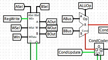
Next, break the connections between the register file and ALU. Set
the ALU's A input to the tunnel ABus, and likewise
set the B input to BBus.
You then need to add the logic to set the values going
into ABus, BBus, and WBus. Create three
more subcircuits, ABus Selector, BBus Selector,
and WIn Selector. These subcircuits take control signals
from the Decoder to determine which values to propagate.
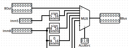
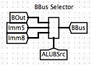
For example, the BBus Selector has within it a mux to
select one of (at least) four values: BOut, Imm5
(sign extended), Imm8 (sign extended), or Imm8
(zero extended). Depending upon your implementation, you may need
additional inputs into the mux.
Likewise, the subcircuit ABus Selector sets ABus using a mux. You will find that AOut is not the only possible value for the ALU's A input.
WIn Selector sets WIn using a mux. The inputs to
this mux are at least ALUOut and DataOut. This mux
is selected by MemToReg, and its output feeds
into WIn.
Hint 1: Note that the ALU does not perform bit
shifting (ash, lsh, or rot),
but a shifted output is one of the possible values
to WIn. The easiest way is to construct a dedicated
subcircuit Logic Operations that takes AOut
and Imm5 to perform the different shift/rotate
operations. You will then need to route this subcircuit's output
back to the main circuit.
Hint 2: Use your spreadsheet from Homework 4.
Part 4: Add Branch Control Logic
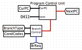
In the third homework, you created the subcircuit PC Control
Unit and added it to Main. Recall that PCSel was
used to select between PC+1 or the constant 411. In this section,
you will build the full PC Control Unit.
-
Study the ULNAv2-B RTN. Create a new
signal
BranchType, a multi-bit value that encodes the various branch types (unconditional, conditional branch if less than, conditional branch if not equal, etc.) -
Create a new subcircuit, Branch Control Unit. This
circuit determines if a branch should be taken or not. It takes
3 inputs:
-
Branch Requested(1 bit) - 1 if a branch is requested, 0 for non-branching instructions.
-
Condition Codes(4 bits) - Current set of condition codes, from the Condition Codes register.
-
Branch Type(multiple bits) - Encoding of branch type, from previous step.
-
-
Integrate your Branch Control Unit into the PC Control Unit,
replacing the old
PCSelcontrol signal with the output from Branch Control Unit. Re-test your main circuit by manually poking the clock line. Each clock cycle should still increment the program counter by 1. -
Remove the constant
411, replacing it with the various possible destinations for a branch instructions. For example, the unconditional branch instructionbjumps toCurPC + SignExtend(Imm11).
Part 5: Finish ULNAv2-B Processor
This part is by far the most difficult part of the entire semester. You are to complete the Instruction Decoder from the fourth homework and tie everything together. You will need to do the following:
-
Add control signals that
set
ALUASrc,ALUBSrc, andMemToReg. -
Decode
Imm5,Imm8, andImm11. Route them to the B Bus and other places throughout. - Generate control signals for your Branch Control Unit.
Hint 3: Some control signals will be obvious. For
example,
MemRead is true when executing ldw
or ldwi instructions. Use your Karnaugh maps from HW4
whenever possible.
Hint 4: Create more Karnaugh maps for the rest of the control signals. Use your spreadsheet to analyze all of the instructions.
Test your decoder thus far with adder.S
and bosrt.S from Homework 4. Load the assembled image into
Instruction Memory, then poke the clock several times. Check that
all signals are generated correctly, and that the program goes into
an infinite loop when it executes the halt
instruction. Compare your circuit's state to what the emulator
reports.
Other Hints and Notes
- Ask plenty of questions on the Blackboard discussion board.
- At the top of your proj2.S, list any help you received as well as web pages you consulted. Please do not use any URL shorteners, such as goo.gl or TinyURL. Also, do not cite shared data services, such as Pastebin, Dropbox, or Google Drive.
- You may use any Logisim component that you can find. If you use a component that does not natively come with Logisim, be sure you cite it.
- You are free to construct your circuit differently than the images above. Specifically, the diagrams above intentionally omitted some control signals.
Extra Credit
You may earn an additional 10% credit for this assignment by making Part 1 easier to grade when run on your circuit. As currently written, the grader must manually inspect the Data Memory after the processor halts, to determine if it holds the correct the number of fizzes and buzzes.
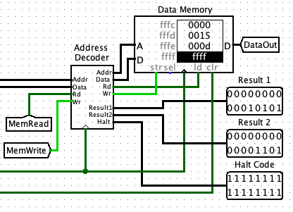
Create a new component, Address Decoder, that sits between
the ALU and Data Memory. In the simple case, it acts as
a passthrough: the input
ports Addr, Data, Rd, and Wr are
simply replicated to similarly named output ports. In addition, it
intercepts writes to these addresses:
| Physical Address | Description |
|---|---|
| 0xfffd | Output to Result1 the most-recently written value to address 0xfffd. The value is still stored into Data Memory. A read from this address goes to Data Memory as normal. |
| 0xfffe | Output to Result2 the most-recently written value to address 0xfffe. The value is still stored into Data Memory. A read from this address goes to Data Memory as normal. |
| 0xffff | Output to Halt the most-recently written value to address 0xffff. The value is still stored into Data Memory. A read from this address goes to Data Memory as normal. |
Observe that if your Part 1 implementation is correct, Result 1 will be the number of fizzes, while Result 2 is the number of buzzes.
If you choose to perform this extra credit, put a comment near the top of your proj2.S, alerting the grader.