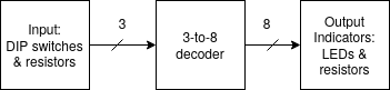
Lab 2 Objective and Overview
In this laboratory, students will learn how to use a datasheet, an integrated circuit, and review the concept of binary codes by converting them to a decimal equivalent. The decimal equivalent is represented with a one-hot encoding. One output is active at a time.
You will use an IC, a 3-to-8 line decoder, as the basis of this lab. DIP (dual inline packaged) switches and resistors will be used to provide inputs. LEDs and resistors will be used as output state indicators.
Concepts and Theory
Integrated Circuit
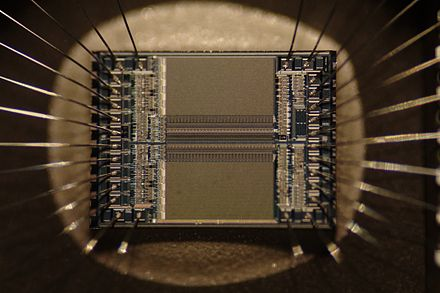
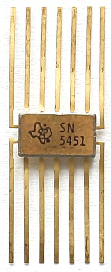
- An Integrated Circuit (also called chip) is an electronic circuit including thousands of millions small transistors, op-amps, capacitors, resistors, and etc. all located on a semiconductor wafer. In the image below, an IC is shown with bonding wires connected to it.
- These are also referred to as "chips," or "microchips."
- These can be Analog, Digital or Mixed Signal
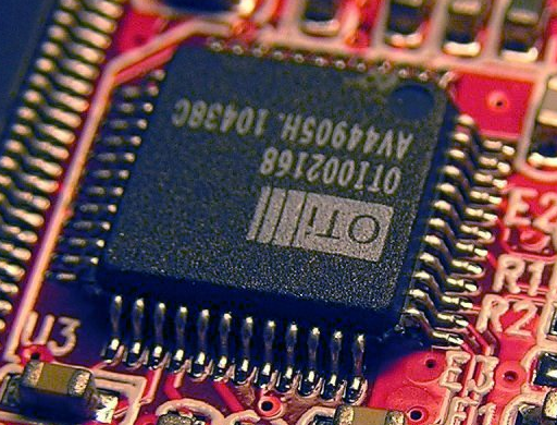
- In the image below the IC can be seen through a window in a package.
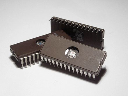
IC Packaging
The following are some common IC packages, which contain the IC, bonding wires and connections to physical pins, as well as mechanical body. The packaging also help dissipate heat away from the IC. Sometimes we say "chip" to referred to the package, and this is understood by the context of use.
- Through Hole:
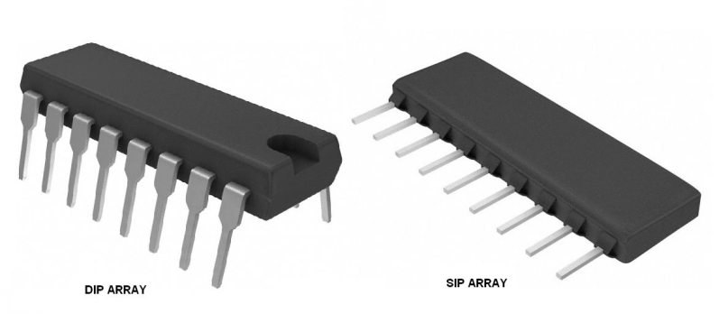
- Single In-Line Package
- Dual In-line Package
- Surface Mount
- Flat
May Other common types of packages exist, including Ball Grid Arrays (BGA), though you would not use those types of packages in this course.
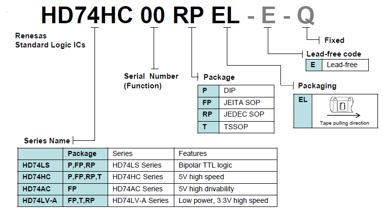
IC Part Numbering scheme
Number Schemes are used to identify parts, families of parts, and variants with different characteristics.
Technical Datasheet:
Technical Datasheet: a document containing the device’s technical characteristics including pin assignment, logic diagram, truth table, and operating details provided by the manufacturer.
- Datasheets for parts used in this course are openly available an indexed by web search engines. To find a datasheet use the following searchstring: "
datasheet”. - Example search: “74HC138AP datasheet”
- Some key information found in datasheet:
- Pinout: shows mapping of physical pins to logic signals
- Logic Diagram: summary depiction (schematic) of underlying circuit
- Truth Table: table depicting function of combinational or squential circuits.
3-to-8 Decoder IC
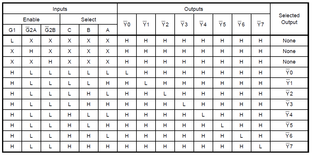
The IC used in this lab decodes three binary weighted address inputs to eight mutually exclusive outputs -- one of this outputs is active at a time. The outputs on this IC are active-low, meaning that the output is driven to a low voltage to indicate when active. The current which drives the output low will be sourced through an LED to turn it on. The IC has additional inputs other than the address pins that need to be set in order to see active outputs.
74HC138AP Pinout/Pin Assignment:
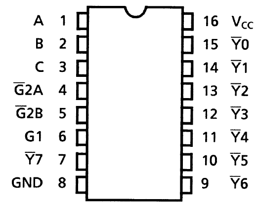
74HC138AP Truth Table:
Voltage and Logic
-
We will use Voltage Logic Levels to assign logical values to the chip’s input pins.
-
In our circuit, the inputs are active high -- small voltages (little difference in potential from GND) will serve as our logical 0, or “low” value, and VCC will be our logical 1, or “High” value.
-
Inputs A, B, and C can be set Low OR High, but the active-low outputs, Y, will change according to the truth table.
-
According to the truth table, and both need to be driven low, and G1 needs to be driven high to see outputs change according to the input address pins CBA
Tips for Beginners working with ICs
- Keep power supply OFF until circuit is finished.
- A heating chip = wrong pin connection!!!
- Use colored wiring standard in your circuits
- VCC = red
- GND = black/blue
- Make inputs a different color than outputs
- Use a multimeter to verify the operation of the input circuitry as well as the voltage at the pins labeled GND and Vcc . You would place the negative probe (black) lead on the ground net and the positive probe (red) lead on the net of interest to see the voltage. Values near 0 voltages considered 0 and values near 5 V are high. Values near the middle of the range might indicate a short or open in the circuit.
Input Generation for this lab:
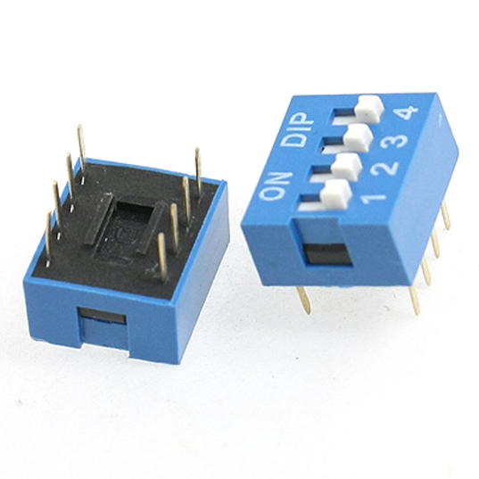
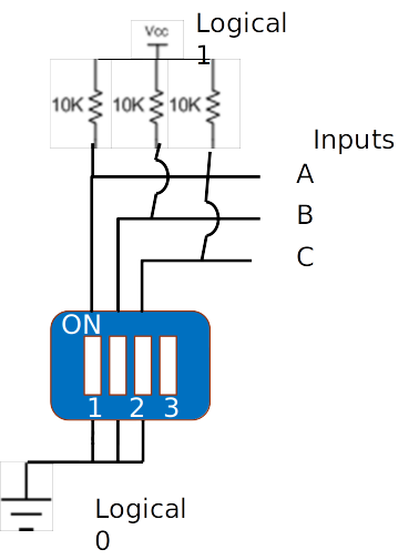
- Inputs A, B, and C will be driven using a DIP switch in combination with a pull-up resistor connected to Vcc. This is shown in the picture below.
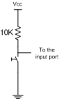
- When "closed" the dip switch pulls the free node between the resistor and switch to ground, representing logical '0'.
- If the switch is opened (disconnected/broken path), the resistor will pull the node high via the resistor connected to Vcc.
- We will need three of these switch circuits, because we have 3 inputs.
- The part used in this lab contains four switches.
How the DIP switch will be used
Outputs Indicators
- You can use an Indicator Circuit built from an LED and current-limiting resistor, as seen in the previous lab.
Required Equipment
- Decoder: a device that converts a number's binary notation to its decimal equivalent.
- Switch: a digital key that allows switching the input port between
0and1. - LED, (330, 1K ohms) resistors, breadboard, power supply, multi-meter.
Experiment and Procedure
- Connect the decoder to the breadboard and wire GND and VCC pins according to the pin assignment (Figure 1).
- Enable the chip by holding the enable input high and enable inputs and, low; otherwise, the chip is disabled and decoding function is inhibited so that all outputs go high. (, , and are used as address decoder in memory systems to ease cascade connections).
- Connect input ports to both GND and VCC by the use of a switch circuit.
- Connect Output ports to the voltage indicator circuits.
- Verify the circuit’s functionality by examining all possible input states and compare with the truth table (Table 1). Fill in the state of each LED in Table .
Table 1 -- 74138 Truth Table
| Inputs | Outputs | ||||||||||||
|---|---|---|---|---|---|---|---|---|---|---|---|---|---|
| Enable | Select | ||||||||||||
| G1 | C | B | A | ||||||||||
| H | L | L | L | L | L | L | H | H | H | H | H | H | H |
| H | L | L | L | L | H | H | L | H | H | H | H | H | H |
| H | L | L | L | H | L | H | H | L | H | H | H | H | H |
| H | L | L | L | H | H | H | H | H | L | H | H | H | H |
| H | L | L | H | L | L | H | H | H | H | L | H | H | H |
| H | L | L | H | L | H | H | H | H | H | H | L | H | H |
| H | L | L | H | H | L | H | H | H | H | H | H | L | H |
| H | L | L | H | H | H | H | H | H | H | H | H | H | L |
Table 2 -- LED Status
| Inputs | Outputs | ||||||||||||
|---|---|---|---|---|---|---|---|---|---|---|---|---|---|
| Enable | Select | ||||||||||||
| G1 | C | B | A | LED0 | LED1 | LED2 | LED3 | LED4 | LED5 | LED6 | LED7 | ||
| H | L | L | L | L | L | _ | _ | _ | _ | _ | _ | _ | _ |
| H | L | L | L | L | L | _ | _ | _ | _ | _ | _ | _ | _ |
| H | L | L | L | L | H | _ | _ | _ | _ | _ | _ | _ | _ |
| H | L | L | L | H | L | _ | _ | _ | _ | _ | _ | _ | _ |
| H | L | L | L | H | H | _ | _ | _ | _ | _ | _ | _ | _ |
| H | L | L | H | L | L | _ | _ | _ | _ | _ | _ | _ | _ |
| H | L | L | H | L | H | _ | _ | _ | _ | _ | _ | _ | _ |
| H | L | L | H | H | L | _ | _ | _ | _ | _ | _ | _ | _ |
| H | L | L | H | H | H | _ | _ | _ | _ | _ | _ | _ | _ |
Lab Instructor Verification _________________________________
Lab Report
This week no lab report is required.